GebraBit

GebraBit ADPD188GG Optical Heart Rate Monitoring and SpO2 measurement sensor Module Overview

متن سربرگ خود را وارد کنید

ماژول ضربان قلب GebraBit ADPD188GG

GebraBit ADPD188GG Optical Heart Rate Monitoring and SpO2 measurement sensor Module Overview

ماژول ضربان قلب GebraBit ADPD188GG
  1. Home
  2. »
  3. Blog
  4. »
  5. GebraBit ADPD188GG Optical Heart Rate Monitoring and SpO2 measurement sensor Module Overview

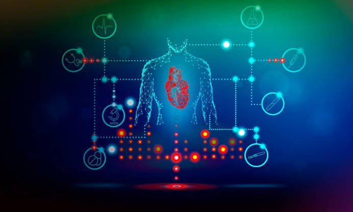
Biomedical sensors are special electronic devices that can transduce biomedical signals into easily measurable electric signals. Biomedical sensors are the key component in various medical diagnostic instruments and equipment.

Biomedical sensors have been widely applied in medical image analysis and diagnostics, portable and clinical diagnostics, and laboratory analytical applications.

Biomedical sensors are usually classified according to the quantity to be measured and are typically categorized as physical, electrical, or chemical, depending on their specific applications.

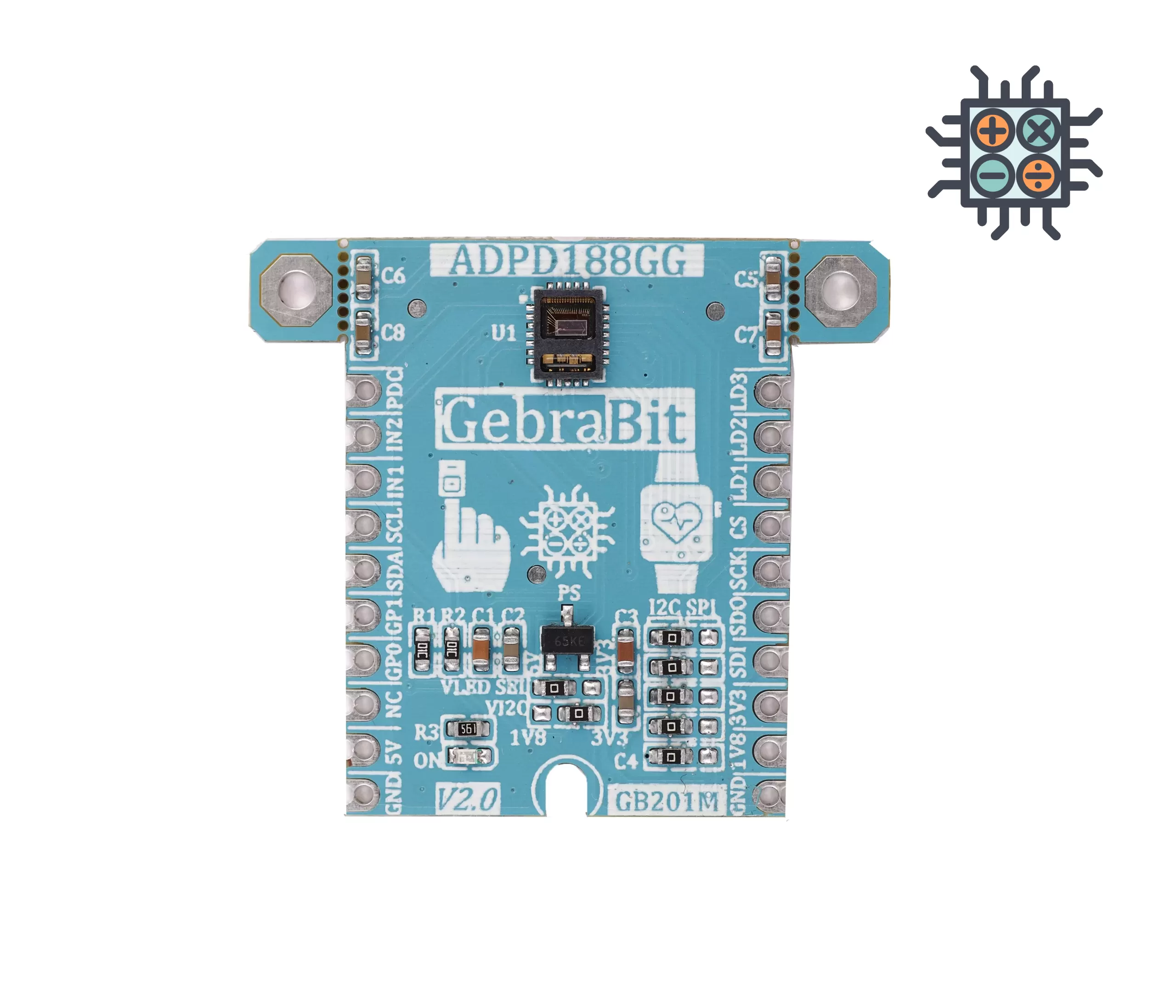
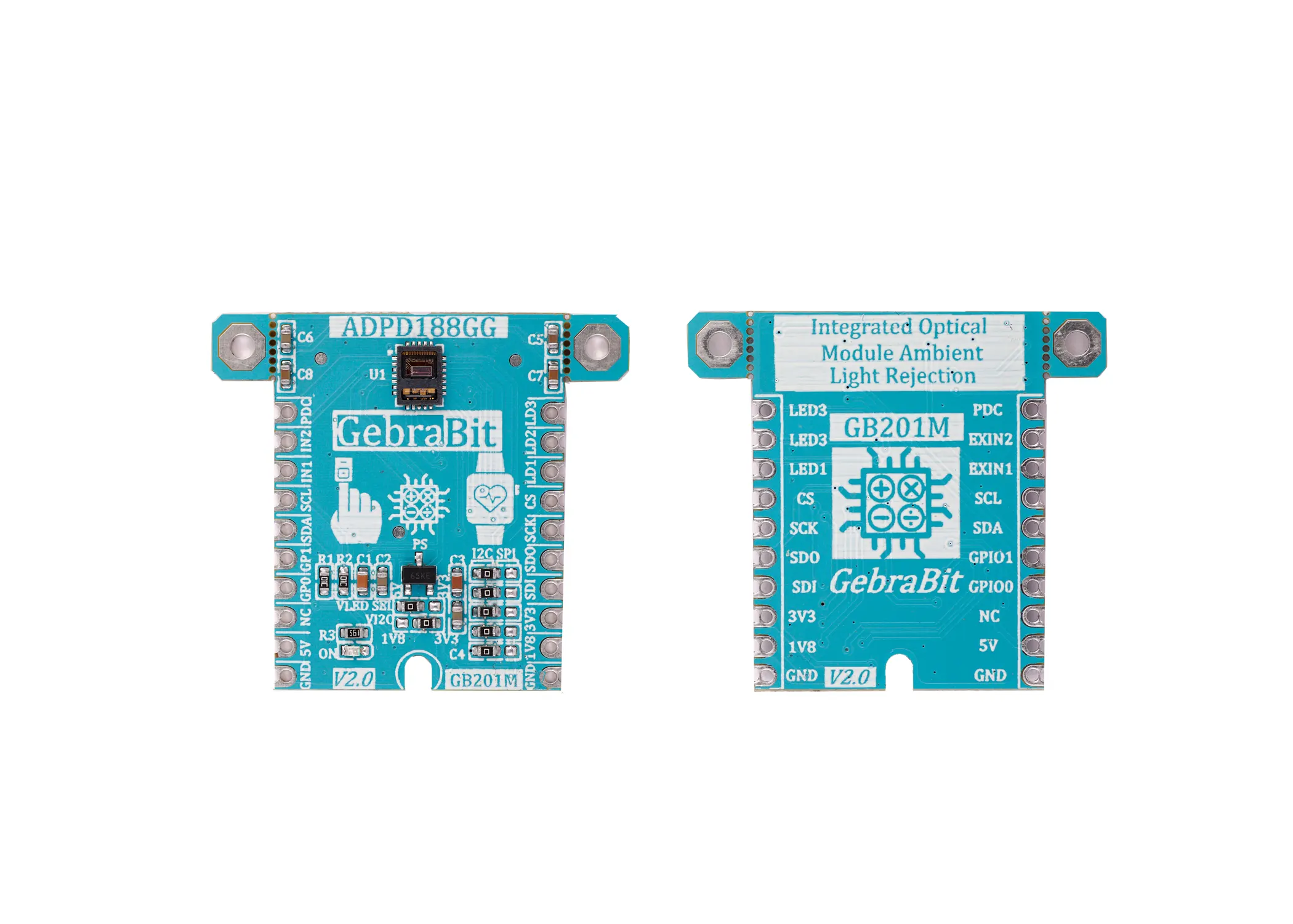
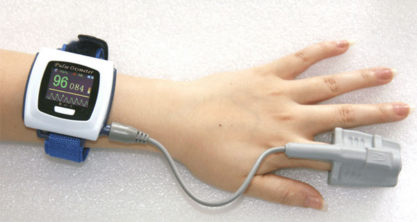
pulse oximeter sensors are small non-invasive devices that are attached to a person’s finger, or other appendages, to measure blood oxygen saturation (SpO2) and heart rate. These sensors determine how efficiently oxygen is being carried through the body by the bloodstream. There are different variations of pulse oximeter sensors that attach to fingers, ears or toes and, in the case of veterinary applications, on the tongue.

Optical heart-rate monitors are the most common pulse sensors in wearables. Most of them glean heart-rate data through “photo plethysmography” (PPG), or the process of using light to measure blood flow. Wearables with optical heart-rate monitors have small LEDs on their undersides that shine green light onto the skin on your wrist. The different wavelengths of light from these optical emitters interact differently with the blood flowing through your wrist. When that light refracts (or reflects) off your flowing blood, another sensor in the wearable captures that information. That data can then be processed, along with motion information detected by the device’s accelerometer, with algorithms to produce understandable pulse readings.

An overview of the ADPD188GG sensor

The ADPD188GG is a complete photometric system designed to measure optical signals from ambient light and from synchronous reflected light emitting diode (LED) pulses. Synchronous measurement offers best-in-class rejection of ambient light interference, both dc and ac. The module integrates a highly efficient photometric front end, two LEDs, and two photodiode (PD).
The front end of the application specific integrated circuit (ASIC) consists of a control block, a 14-bit analog-to-digital converter (ADC). The control circuitry includes flexible LED signaling and synchronous detection.
The analog front end (AFE) features best-in-class rejection of signal offset and corruption due to modulated interference commonly caused by ambient light.

Specification

Applications

  • Output type: Digital – SPI and I2C
  • ADC Resolution: 14 Bit
  • Type of filter: IR cut filter
  • Wavelength Peak: Green: 525nm PD1: 0.4nm PD2: 0.8nm

For more specifications, please refer to datasheet

  • Optical heart rate monitoring
  • Reflective SpO2 measurement
  • CNIBP measurement

ADPD188GG module Key Features

  • User-selectable I2C logic level voltage
  • User-selectable ADPD188GG Green LED Anode Supply Voltage
  • User-selectable interface protocol (I2C or SPI)
  • 1V8 Voltage Regulator
  • 1V8 Output Voltage
  • On Board, ON/OFF LED indicator
  • Pin Compatible with GEBRABUS
  • Access to all important I/O of ADPD188GG
  • It can be used as a daughter board of GEBRABIT MCU Modules
  • Featuring Castellated pad (Assembled as SMD Part)
  • Separatable screw parts to reduce the size of the board
  • Package: GebraBit small (36.29mm x 32.72mm)

GebraBit ADPD188GG module

GebraBit ADPD188GG is an integrated Optical Module with Ambient Light Rejection with 2 green LEDs, and 2 PDs with IR cut filter.

GebraBit ADPD188GG module, due to an integrated 1V8 regulator, needs a 5V input Supply Voltage to turn the ADPD188GG sensor ON.

Users can interface with GebraBit ADPD188GG by either I2C or SPI protocol. This is achieved by five dedicated  selector jumpers on the bottom right of the GebraBit ADPD188GG module.

 the user needs a starter circuit and driver for hardware development and of course software development of the sensor. For the convenience of users, this work has been done by implementing the ADPD188GG sensor circuit and providing access to the communication and power supply signal pins by GebraBit team.  

It is enough to put the GebraBit ADPD188GG  module in the BreadBoard, then by applying the proper voltage, connect the GebraBit ADPD188GG module with any of the Arduino, Raspberry Pi, Discovery boards, and especially we recommend using GebraBit microcontroller development modules to develop the sensor and receive data.  

The reason for our recommendation when setting up the GebraBit ADPD188GG module with GebraBit microcontroller development modules (such as GebraBit STM32F303 or GebraBit ATMEGA32), is the presence of an internal 3V3 regulator on these modules and the compatibility of the pin order of all GebraBit modules together (GEBRABUS standard). It’s enough to put the GebraBit ADPD188GG module in the corresponding socket as shown in the above picture and develop the desired sensor module without the need for wiring.

Note: Considering that the PA14 pin of the GebraBit STM32F303 microcontroller module is used to program the microcontroller, I2C setting on the PA14 and PA15 pins is impossible in this version, so in this version for  I2C  connection with the GebraBit STM32F303 microcontroller module, GebraBit ADPD188GG module cannot be placed on it as Pin to Pin. For convenience, you can select the SPI protocol by using the on-board jumpers and then place the GebraBit ADPD188GG module as Pin to Pin on the GebraBit STM32F303 module. 

Introduction of module sections

ADPD188GG sensor

It’s the main IC of the following module, which its circuit is designed and  is placed on top of the module and is in charge of optical heart  rate monitoring  and SPO2 measurement.

Communication protocol selection jumpers

If the 0R resistors of all Jumper Selectors are to the left side, the I2C protocol is selected.

If the 0R resistors of all Jumper Selectors are to the left side, the I2C protocol is selected.

by default,I2C protocol is selected.

VI2C selector jumper

According to the state of 0R resistance of this jumper the I2C  logic level voltage of module can be selected  between “1V8” or “3V3”.

LED voltage selector jumper (VLED SEL)

According to the state of 0R resistance of “VLED SEL” jumper, the ADPD188GG  Green LED Anode Supply Voltage can be selected between “5V” or “3V3” .

“1.8V” XC6206P182MRG regulator

In order to achieve 1V8 voltage of the I2C interface logic level, a 1.8V XC6206P182MR-G regulator is used on the GebraBit ADPD188GG module. Due to the existence of this regulator, 5V supply voltage is needed to activate the module sensor.

power supply LED

By applying voltage to the module via the corresponding pin, this LED will be lit.

GebraBit ADPD188GG Module pins

Supply pins

  • 1V8 and 3V3 and 5V: These pins can provide the main power supply of the sensor and LED Anode Supply Voltage and the logic level of the sensor digital connection (I2C or SPI) according to the “VI2C SEL” and “VLED SEL” jumpers state.
  • GND: This is the common ground pin for power the module.

I2C pins

  • By using the on-board embedded Jumper selectors, you can choose the type of module communication  . If the 0R resistors of all the Jumper Selectors are to the left side, the I2C protocol is selected.

    • SDA: This pin is the I2C communication data pin, which is connected to the corresponding data pin in the microcontroller (processor). According to the state of the “VI2C SEL” jumper, you can use the logic level with a voltage of “1V8” or “3V3”.This pin is pulled up with a resistor.
    • SCL: This pin is the I2C communication clock pin, which is connected to the corresponding clock pin in the microcontroller (processor). Depending on the state of the “VI2C SEL” jumper, you can use the logic level with a voltage of 1V8 or 3V3. This pin is pulled up with a resistor.

SPI pins

The type of communication with the module can be selected by using the on-board embedded Jumper Selectors. If the 0R resistors of all the Jumper Selectors are to the right side, the SPI protocol has been selected.

    • SDI (MOSI): This pin is used to send data from the microcontroller (processor) to the module (sensor). The abbreviation of this pin is derived from the Latin phrase Serial Data In / Microcontroller Out Sensor In.
    • SDO (MISO): This pin is used to send data from the module (sensor) to the microcontroller (processor). The abbreviation of this pin is derived from the Latin phrase Serial Data Out / Microcontroller In Sensor Out.
    • SCK: This pin is the clock pin for SPI communication, which is considered as an input for the sensor and is connected to the corresponding clock pin in the microcontroller (processor).
    • CS: This pin is the Chip Select pin for SPI communication with the module (sensor), which is selected by applying LOW voltage (0V), the module (sensor) for SPI communication. This pin is input type for the sensor.

If you want to use several GebraBit ADPD188GG  modules at the same time, it is enough to connect the SDO, SDI, SCK pins of all modules and the microcontroller (processor) and assign a unique pin to each CS.

Other pins

GP0 and GP1: These pins are the GPIO0 and GPIO1  pins of the module, which can be used as general-purpose input/output pins.

IN1 and IN2: These pins are the External analog current input pins.

PDC: this pin is Photodiode Common Cathode Bias pin.

LD1 and LD2 and LD3: These pins are the LED1, LED2 and LED3 Driver Current Sink pins.

Connect to the processor

I2C connection with GebraBit STM32F303

First, make sure that the I2C protocol is selected by using the on-board jumpers, then for i2c communication of GebraBit ADPD188GG and GebraBit STM32F303 microcontroller module, after defining “SDA” and “SCL” on pins PB9 and PB8 (for convenience in STMCUBEMX), follow the below steps:

  • Connect the “3V3” pin of the ADPD188GG module to the “3V3” output pin of the microcontroller module. (red wire)
  • Connect the “GND” pin of the ADPD188GG module to the “GND” pin of the microcontroller module (black wire).
  • Connect the “SCL” pin of the ADPD188GG module to the PB8 pin of the microcontroller (SCL) module (blue wire).
  • Connect the “SDA” pin of the ADPD188GG module to the PB9 pin of the microcontroller (SDA) module. (yellow wire)

You can see how to connect the above mentioned steps in this picture:

SPI connection with GebraBit STM32F303

First, make sure that the SPI protocol is selected by using the on-board jumpers, then for connecting GebraBit ADPD188GG module to the GebraBit STM32F303 microcontroller module with SPI protocol, after defining “SDI”, “SDO”, “SCK”, and “CS” on pins PB5, PB4, PB3, and PC13 ( For ease of work in STMCUBEMX) place the GebraBit ADPD188GG module Pin to Pin on the GebraBit STM32F303 module easily.Here for better understanding the separate connection of these two modules is shown.

SPI or I2C connection with GebraBit ATMEGA32A

Considering that the SPI and I2C pins of the ATMEGA32A microcontroller are based on the GEBRABUS standard and correspond to the SPI and I2C pins of other GEBRABIT modules, the GebraBit ADPD188GG module can be placed pin to pin  on the GebraBit ATMEGA32A module and communicate with the GebraBit ADPD188GG  module via SPI or I2C by changing the state of the protocol selection jumper resistors.Here for better understanding the separate connection of these two modules is shown.

I2C Connection
SPI Connection

NOTE: If you are using GebraBit microcontroller modules, note that the power selector jumpers of the GebraBit ADPD188GG  are set to 3V3 so that you can easily power-on the GebraBit ADPD188GG  module by getting the 3V3 voltage from the microcontroller module.

I2C Connection with ARDUINO UNO

First, make sure that the I2C protocol is selected by using the on-board jumpers, then follow the below steps to connect the GebraBit ADPD188GG module to the ARDUINO UNO via I2C :

  • Connect the “3V3” pin of the ADPD188GG module to the “3V3” output pin of the ARDUINO UNO board. (red wire)
  • Connect the “GND” pin of the ADPD188GG module to the “GND” pin of the ARDUINO UNO board (black wire).
  • Connect the “SCL” pin of the ADPD188GG module to the A5 pin of the ARDUINO UNO board (SCL). (blue wire)
  • Connect the “SDA” pin of the ADPD188GG module to the A4 pin of the ARDUINO UNO board (SDA). (orange wire)

You can see how to connect the above mentioned steps in this picture:

SPI Connection with ARDUINO UNO

First, make sure the SPI protocol is selected using the on-board jumpers, then follow the below  steps to connect the GebraBit ADPD188GG module to the ARDUINO UNO via SPI:

  • Connect the “3V3” pin of the ADPD188GG module to the “3V3” output pin of the ARDUINO UNO board. (red wire)
  • Connect the “GND” pin of the ADPD188GG module to the “GND” pin of the ARDUINO UNO board (black wire).
  • Connect the “SDI” pin of the ADPD188GG module to the D11 pin of the ARDUINO UNO board (SDI). (yellow wire)
  • Connect the “SDO” pin of the ADPD188GG module to the D12 pin of the ARDUINO UNO board (SDO). (Purple wire)
  • Connect the “SCK” pin of the ADPD188GG module to the D13 pin of the ARDUINO UNO board (SCK). (Orange wire)
  • Connect the “CS” pin of the ADPD188GG module to the D10 pin of the ARDUINO UNO board (SS). (blue wire)

You can see how to connect the above mentioned steps in this picture:

این مقاله را با دوستانتان به اشتراک بگذارید!

Leave a Reply

Your email address will not be published. Required fields are marked *

Shopping cart
Start typing to see posts you are looking for.

Sign in

No account yet?